Analysis and Design of Passive Microwave Devices in Planar and Hybrid (SIW waveguides) Technology
The group has also capabilities for analysis and design of passive microwave circuits implemented in planar technology (microstrip and coplanar), as well as in the promising hybrid technology of substrate integrated waveguide (SIW), both widely used in the areas of mobile (GSM and UMTS), wireless (LMDS, MVDS and FWA) and spatial (input stage) communications. Under this R & D line the following activities are carried out:
- Development of new rigorous and efficient electromagnetic analysis methods (full-wave) for planar and SIW technology based components, based on hybrid methods that combine modal adaptation (mode-matching) and integral equation (Method of Moments and BI-RME 2D) techniques.
- Practical operation of full-wave electromagnetic analysis commercial programs (there are available licenses for ANSYS Designer, Ansoft HFSS and COMSOL Multiphysics) for practical design (combining circuit synthesis methods and advanced optimization algorithms) of high frequency passive components in planar and SIW technologies (eg filters with advanced responses and transitions).
- Optimized design using aggressive space mapping techniques (combining circuital equivalent models with commercial EM simulators) of new transmission lines and compact devices (filters, splitters and hybrids) based in metamaterials (left-handed). These devices (see filter in coplanar technology in photos) are based on transmission lines loaded with CL type resonant circuits or resonant rings (SRR).
- Practical design, including prototypes manufacturing (with own facilities at the UPV, see photos) and experimental measurements of passive devices (filters, diplexers and multiplexers, power dividers, couplers and hybrids, and antenna feed networks) in planar and hybrid technologies for high frequency (microwave) communications systems.
- Prediction of RF discharge effects (multipaction and corona) in planar devices to be used in space applications, combining full-wave EM simulation and particle physics algorithms. Making use of the group facilities, and the facilities shared with the European Space Agency and the Val Space Consortium, experimental measurements are made of these RF discharge phenomena.
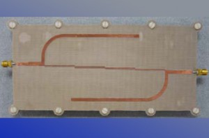 NRN Microstrip Filter |
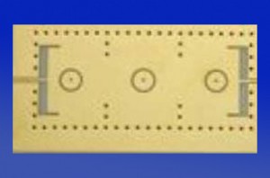 Combline SIW filter |
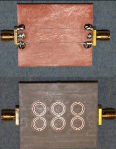 SRR Cband Filter |
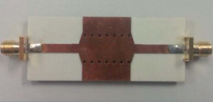 Microstrip SIW transition |
| SRR Cband Filter |
The different activities related to these planar and SIW technologies have available the EM simulation and experimental measurement facilities as previously described (shared with the above R&D line focused on waveguide technology), as well as an own manufacturing facility for these compact devices that comprises (see photos below): S103 LPKF micromilling machine, galvanic plating system for drilling holes (vias) in planar and waveguide SIW circuits, LPKF reflow oven for welding and metallization processes, and LPKF SMD (Surface Mounting Devices) pick and place machine.
With the aim of measuring integrated and/or compact circuits directly on substrate (either dielectric or semiconductor wafer), the group has also a probe station (model Cascade Microtech) for positioning and measurement.
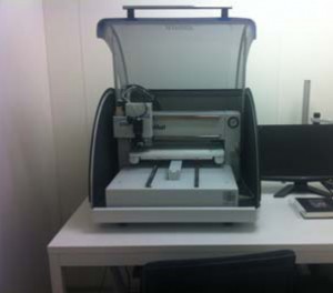 Milling Machine |
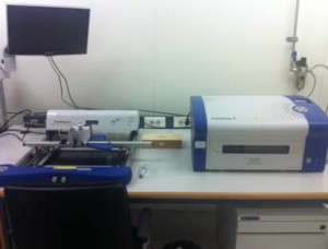 Pick Place |
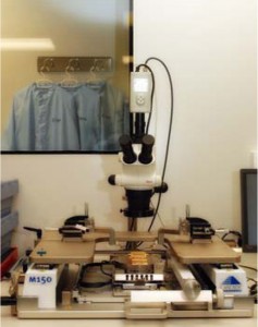 Measurement Station |
 Measurement Station |

